 English
- English
-
 Español
 -
 Português
 -
 русский
 -
 Français
 -
 日本語
日本語 -
 Deutsch
 -
 tiếng Việt
 -
 Italiano
 -
 Nederlands
 -
 ภาษาไทย
 -
 Polski
 -
 한국어
한국어 -
 Svenska
 -
 magyar
 -
 Malay
Malay -
 বাংলা ভাষার
 -
 Dansk
Dansk -
 Suomi
Suomi -
 हिन्दी
 -
 Pilipino
 -
 Türkçe
 -
 Gaeilge
 -
 العربية
 -
 Indonesia
 -
 Norsk
Norsk -
 تمل
تمل -
 český
český -
 ελληνικά
 -
 український
 -
 Javanese
 -
 فارسی
فارسی -
 தமிழ்
தமிழ் -
 తెలుగు
 -
 नेपाली
 -
 Burmese
 -
 български
 -
 ລາວ
ລາວ -
 Latine
 -
 Қазақша
 -
 Euskal
 -
 Azərbaycan
 -
 Slovenský jazyk
 -
 Македонски
 -
 Lietuvos
 -
 Eesti Keel
 -
 Română
 -
 Slovenski
 -
 मराठी
मराठी -
 Srpski језик


The principle of vacuum coating is revealed: technical foundation, process flow, and industry application
2024-07-05
It is a process of depositing materials onto a substrate surface using physical or chemical methods in a low-pressure environment to form a thin film. Through this technology, high-purity and high-precision thin film deposition can be achieved, giving it specific optical, electrical, mechanical and other properties. Therefore, vacuum coating has important application value in modern industry. For example, in semiconductor manufacturing, vacuum coating is used to produce various functional layers on wafers; In the field of optics, anti reflection and anti reflection effects can be achieved through coating; In mechanical manufacturing, vacuum coating can improve the wear resistance and corrosion resistance of components.
Basic Theory of Vacuum Coating
A. Fundamentals of Vacuum Technology
1. Definition and measurement of vacuum
Vacuum refers to a gas environment below one atmospheric pressure (760 millimeters of mercury, 101325 Pa). According to the different degrees of vacuum, vacuum can be divided into low vacuum, medium vacuum, high vacuum, and ultra-high vacuum. The measurement of vacuum degree is usually carried out using pressure gauges, such as MacLehose pressure gauges, Pirani gauges, and cold cathode gauges.
2. Vacuum acquisition method
Mechanical pump: Mechanical pumps discharge gas through mechanical movement, commonly including rotary vane pumps and diaphragm pumps. These pumps are suitable for obtaining low and medium vacuum.
Molecular pump: A molecular pump utilizes a high-speed rotating rotor to mechanically expel gas, suitable for obtaining high and ultra-high vacuum.
Turbopump: Turbomolecular pump combines the advantages of mechanical pump and molecular pump, achieving efficient pumping through multi-stage rotating blades, and is widely used in high vacuum systems.
B. Thin film physics
Classification and basic properties of thin films
According to the preparation method and purpose, thin films can be divided into metal films, ceramic films, polymer films, etc. The basic properties of thin films include thickness, uniformity, adhesion, hardness, optical properties (such as transmittance and reflectivity), and electrical properties (such as conductivity and dielectric constant).
The basic process and mechanism of thin film growth
The growth process of thin films usually includes stages such as nucleation, island growth, contiguous and layered growth. Nucleation is the initial stage in which atoms or molecules gather on the substrate surface to form small islands; As time goes by, these small islands gradually connect into sheets, eventually forming a continuous thin film. The growth mechanism is influenced by factors such as material properties, substrate surface state, deposition temperature, and deposition rate.
C. Fundamentals of Materials Science
Common Coating Materials and Their Characteristics
Common coating materials include metals (such as aluminum, gold, platinum), semiconductors (such as silicon and germanium), ceramics (such as aluminum oxide and silicon nitride), and organic materials (such as polymers). Different materials have different physical and chemical properties, and when selecting coating materials, their performance requirements in specific applications need to be considered.
Principles and standards for material selection
The principles of material selection include chemical stability, mechanical properties, optical properties, and electrical properties. Standards usually involve the purity, particle size, impurity content, etc. of materials to ensure the quality and functional characteristics of thin films.
The main methods and principles of vacuum coating
A. Physical Vapor Deposition (PVD)
Overview and classification
Physical vapor deposition (PVD) is a technique that utilizes physical processes to deposit materials onto the substrate surface. The main categories include evaporation coating, sputtering coating, and ion plating.
Specific process principles and steps
Evaporative coating: The material evaporates at high temperature and deposits a thin film on the substrate through a vacuum system. Common heat sources include resistance heating and electron beam heating.
Sputtering coating: By bombarding with inert gas ions, the target material atoms are sputtered onto the substrate to form a thin film. Common methods include DC sputtering and RF sputtering.
Ion plating: Under the action of an ion source, ionized materials are accelerated to deposit onto the substrate, commonly used to prepare high hardness coatings.
Advantages, disadvantages, and scope of application
The advantages of PVD technology include thin film density, strong adhesion, and low process temperature
, but the equipment is complex and the cost is high. Suitable for the preparation of metal, alloy, and ceramic thin films, widely used in the fields of electronics, optics, and decoration.
B. Chemical Vapor Deposition (CVD)
The basic concept of CVD
Chemical vapor deposition (CVD) is a technique of depositing thin films on a substrate surface through chemical reactions. The reaction gas decomposes or undergoes chemical reactions at high temperatures, generating solid deposits.
Various CVD methods
Low pressure CVD (LPCVD): Reacts in a low pressure environment, with high film quality and good uniformity, suitable for the semiconductor industry.
Plasma Enhanced CVD (PECVD): Utilizing plasma to accelerate chemical reactions and reduce reaction temperature, suitable for temperature sensitive materials.
Metal Organic Chemical Vapor Deposition (MOCVD): Using metal organic compounds as precursors, it is suitable for preparing complex compound thin films, such as III-V semiconductor materials.
Process characteristics and application examples
The characteristics of CVD process are dense film, high purity, and good uniformity, but high temperature and complex equipment. Widely used in semiconductor devices, solar cells, optical coatings and other fields.
C. Atomic layer deposition (ALD)
The unique mechanism and steps of ALD
Atomic layer deposition (ALD) is a technique that precisely controls the thickness of thin films by alternately supplying precursor gas and reaction gas, and depositing atomic layers layer by layer on the substrate surface. Its unique self limiting reaction mechanism allows for precise control of film thickness to the nanoscale.
Comparison with PVD and CVD
Compared with PVD and CVD, the advantages of ALD lie in precise control of film thickness, high uniformity, and strong ability to cover complex structures. However, the deposition speed is slower, making it suitable for applications that require extremely high precision and uniformity.
application prospect
ALD technology has broad application prospects in fields such as microelectronics, nanotechnology, and biomedicine, such as the preparation of high k dielectric films, nanowires, and biosensors.
Vacuum coating equipment and process flow
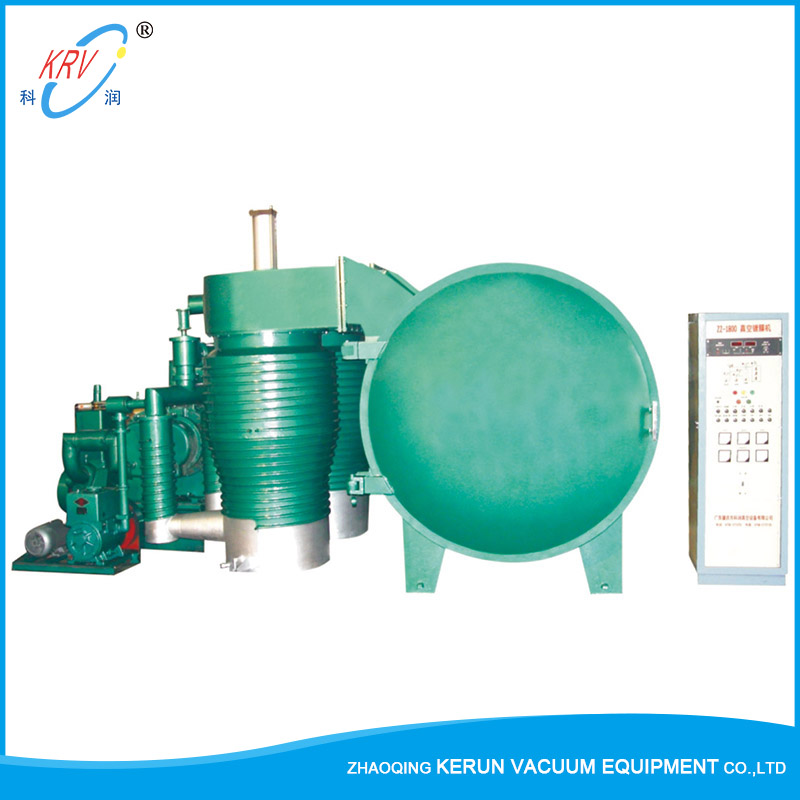
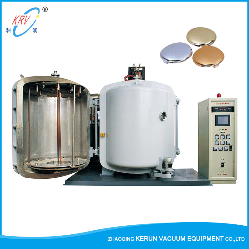
A. Typical vacuum coating equipment
The basic structure of the coating machine
Typical coating equipment includes vacuum chambers, extraction systems, heating systems, control systems, and coating sources. The vacuum chamber provides a low-pressure environment, the pumping system is used to obtain and maintain vacuum, the coating source provides materials, and the control system monitors and adjusts process parameters.
Common device types
Evaporative coating machine: The material is evaporated and deposited onto the substrate through resistance heating or electron beam heating.
Sputtering coating machine: The target material atoms are sputtered onto the substrate through magnetron sputtering or radio frequency sputtering.
Ion plating equipment: Utilizing an ion source to generate high-energy ion beams to deposit thin films, commonly used in the preparation of hard coatings.
B. Process flow
Pre processing process
Before coating, the substrate surface needs to be cleaned and pretreated to remove surface pollutants and oxide layers, ensuring the adhesion and uniformity of the film. Common methods include ultrasonic cleaning, chemical cleaning, and plasma cleaning.
Coating process
The key to the coating process is the optimization of control parameters, including vacuum degree, temperature, gas flow rate, and deposition rate. These parameters directly affect the quality and performance of the film.
Post processing process
The film after coating often requires post-treatment, such as annealing and passivation, to improve the physical and chemical properties and stability of the film.
C. Process control and optimization
Control of parameters such as vacuum degree, temperature, atmosphere, etc
By precisely controlling the vacuum degree, deposition temperature, and gas composition, the growth process of thin films can be optimized, and the uniformity and performance of the films can be improved.
Control of coating thickness and uniformity
By using online monitoring technologies such as quartz crystal microbalance and optical monitoring system, real-time monitoring and control of coating thickness and uniformity can be achieved to ensure the quality of the film.
Quality testing and evaluation methods
The detection of film quality includes the evaluation of physical, chemical, and mechanical properties, such as film thickness, surface morphology, composition analysis, adhesion, hardness, etc. Common methods include scanning electron microscopy (SEM), atomic force microscopy (AFM), X-ray diffraction (XRD), and spectroscopic analysis.
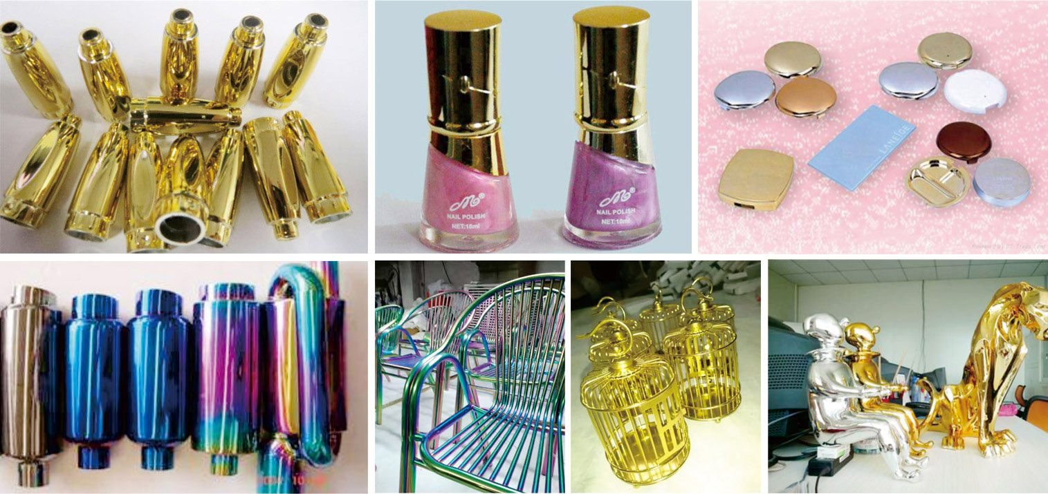
Application examples of vacuum coating
A. Electronics and semiconductor industry
Integrated Circuit Manufacturing
Vacuum coating technology is used in integrated circuit manufacturing to deposit metal interconnect layers, insulation layers, and protective layers. The high-precision coating process ensures circuit performance and reliability.
Coating technology for displays and sensors
In display manufacturing, vacuum coating is used to deposit transparent conductive films and optical films; In sensor manufacturing, coating technology is used to prepare sensitive components and protective layers, improving the sensitivity and durability of sensors.
B. Optics and Optoelectronics
Types and applications of optical thin films
Optical thin films include anti reflective films, anti reflective films, filter films, and reflective films. By precisely controlling the thickness and optical properties of the films, specific optical effects can be achieved, such as reducing reflection, enhancing transmittance, and selective filtering.
The application of coating in lasers and optical devices
In lasers and optical devices, vacuum coating technology is used to manufacture high-performance mirrors, windows, and lenses, improving the efficiency and stability of optical systems.
C. Mechanical and protective applications
Hard coating and wear-resistant coating
Hard coatings and wear-resistant coatings are prepared through vacuum coating technology and widely used in tools, molds, and mechanical parts to improve their wear resistance and service life.
Application of anti-corrosion coatings
Anti corrosion coatings deposit a layer of corrosion-resistant materials, such as chromium and titanium, on the metal surface through vacuum coating technology to enhance its corrosion resistance and extend the service life of the equipment.
D. Applications in emerging fields
Vacuum coating in nanotechnology
In nanotechnology, vacuum coating is used to prepare nanoscale structures and thin films, such as nanowires, nanoparticles, and quantum dots, applied in fields such as electronics, optoelectronics, and catalysis.
Biomedical applications
Vacuum coating technology is used in biomedical applications to manufacture functional coatings on biocompatible films, sensors, and medical device surfaces, improving their performance and safety.


X
We use cookies to offer you a better browsing experience, analyze site traffic and personalize content. By using this site, you agree to our use of cookies.
Privacy Policy